The Limits of Photolithography - Questions from reading The Future of Computing by Matz
光刻机的极限--读《代码的未来》产生的疑问
I recently finished reading "The Future of Computing" by Yukihiro Matsumoto (Matz), a book published by Matz in 2012. Although ten years have passed since its publication, some of the technologies mentioned in the book have disappeared and some of the "future" has been realized, it is still a rewarding read in this era.
The Future of Computing focuses on what programming will look like 20 or 100 years from now. To answer this question, the update of computer hardware is a factor that must be taken into account. For the past 40 years, Moore's Law has been in play. But the increase in chip integration seems to be approaching its physical limits.
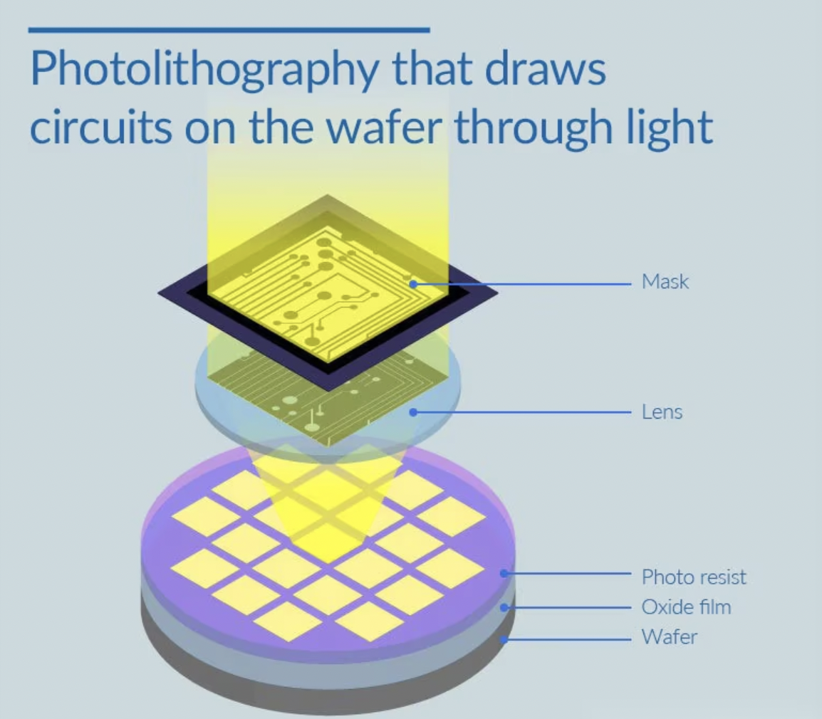
The current large-scale integrated circuit (LSI) is still using photolithography to etch the circuit "painted" on the wafer. When the width of the circuit is reduced to tens of nanometers or even a few nanometers, various problems arise. If such a circuit exists, then how to keep the circuit insulation, dealing with heat generation have become problems. But before that, how we make such a circuit by photolithography is a huge challenge in itself - when the size of the image to be imaged is smaller than the wavelength of light, the circuit cannot be printed clearly. Visible light has a wavelength of 380 - 750 nm, so the recent 9 nm process LSIs cannot be fabricated with visible light.
In the section "Moore's Law" in Chapter 6 of "The Future of Code", I encountered this paragraph.
In a forest, the shadow cast by sunlight on the ground through the dense foliage becomes blurred, and it is impossible to distinguish a single leaf. Similarly, when the pattern is smaller than the wavelength of light, it happens that it is blurred and cannot be clearly sensed. In order to be able to print a circuit whose size is smaller than the wavelength of light, people have used a variety of methods, such as filling the lens and wafer with pure water to shorten the wavelength of light, but the limit will come sooner or later. The next step, I'm afraid, will be the use of shorter wavelengths of far ultraviolet or X-rays. But the wavelength is too short, the lens will not be able to use -- it is very difficult to deal with this situation. Perhaps a reflector can be used to replace the lens but the exposure mechanism will become very large, and the cost will rise.
Although it is only one natural segment, it raises many questions for me:
- Why is it said that the wavelength of light can be shortened by filling pure water between the lens and the wafer? I guess it is using refraction (i.e. the speed of light is different in different media). But after the light leaves the pure water, the wavelength should be restored. Then this process does not shorten the wavelength of light.
- When using a shorter wavelength of light, why the lens can not be used? Is it a problem with the process of glass making?
- Based on Question 2, why can a reflector be used instead of a refractor at this time? How can reflection be done to shrink the beam of light? Why is the reflector very large?
This article is to record the process of my exploration of these three questions.
With these questions in mind, I asked my friend David, who is a professor of optics, for advice. One of the more surprising things about the exchange was that the knowledge I learned about chemical analysis during my undergraduate years actually helped.
First was the first question about filling pure water to shorten the wavelength of light. This question told me that I can't imagine from thin air, or I have to see what the actual lithography machine looks like.
As shown in the picture, after the light passes through the mask with the circuit template on top, it passes through the lens, and then the circuit is etched on the wafer. And how exactly is pure water put in?
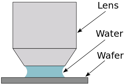
There is actually a technical term for using pure water as a filler, immersion lithography. The light reaches the wafer directly after leaving the water, there is no gap in between, and there is no problem with wavelength recovery after the light leaves the water.
Regarding the second question, why the lens does not work when using far ultraviolet light? If you ask a chemical analyst, he will tell you that glass absorbs ultraviolet light.
Why does glass absorb far ultraviolet light? This is answered in two ways, one is the principle of UV absorption and the other is the material of the glass itself.
There are different forms of motion within a molecule (valence electron motion, vibration, rotation), and together these represent the energy of the molecule. When a molecule absorbs energy from the outside world (e.g., absorption of UV light), it can cause a jump in the energy level of the molecule; and the energy state of the molecule has a quantum character, it can only be at a specific energy level (not a continuous energy state), i.e., the molecule can only absorb the energy of the difference between two energy levels::
$$$ \Delta E = E_2 - E_1 = hv = \frac{hc}{\lambda} $$$
And the main component of the glass is Silicon Dioxide ($SiO_2$) with an energy band (bandgap) of about $8.9 eV$.
Known the Planck constant $ h = 6.624 \times 10^{-34} J \cdot s = 4.136 \times 10^{-15} eV \cdot s $
and the speed of light $ c = 2.998 \times 10^{10} cm\cdot s^{-1} $
Then the wavelength of light that can be absorbed by Silicon Dioxide is
\begin{align*} \lambda &= \frac{hc}{\Delta E} = \frac{4.136 \times 10^{-15} eV \cdot s \times 2.998 \times 10^{10} cm\cdot s^{-1} }{8.9 eV} \\ &= 1.39 \times 10^{-5} cm \\\ &= 139 nm \end{align*}
But in fact, glass contains other impurities besides Silicon Dioxide, such as sodium oxides, which can make the UV absorption not just at the point of 139 nm, but at a nearby wavelength.
The far ultraviolet (F-UV) wavelength lies between 122 - 200 nm, which is just inside the absorption range of Silicon Dioxide. Therefore, glass is transparent to the human eye and does not absorb visible light, but it can absorb far-UV light. It is difficult to use a glass lens alone for lithography without other changes.
The third question is why a reflector can be used instead of a lens, and why this increases the size.
This is really a matter of optical path design. We use a lens for the purpose of focusing light. But in addition to lenses, we can also use concave mirrors (parabolic mirrors) to focus light.
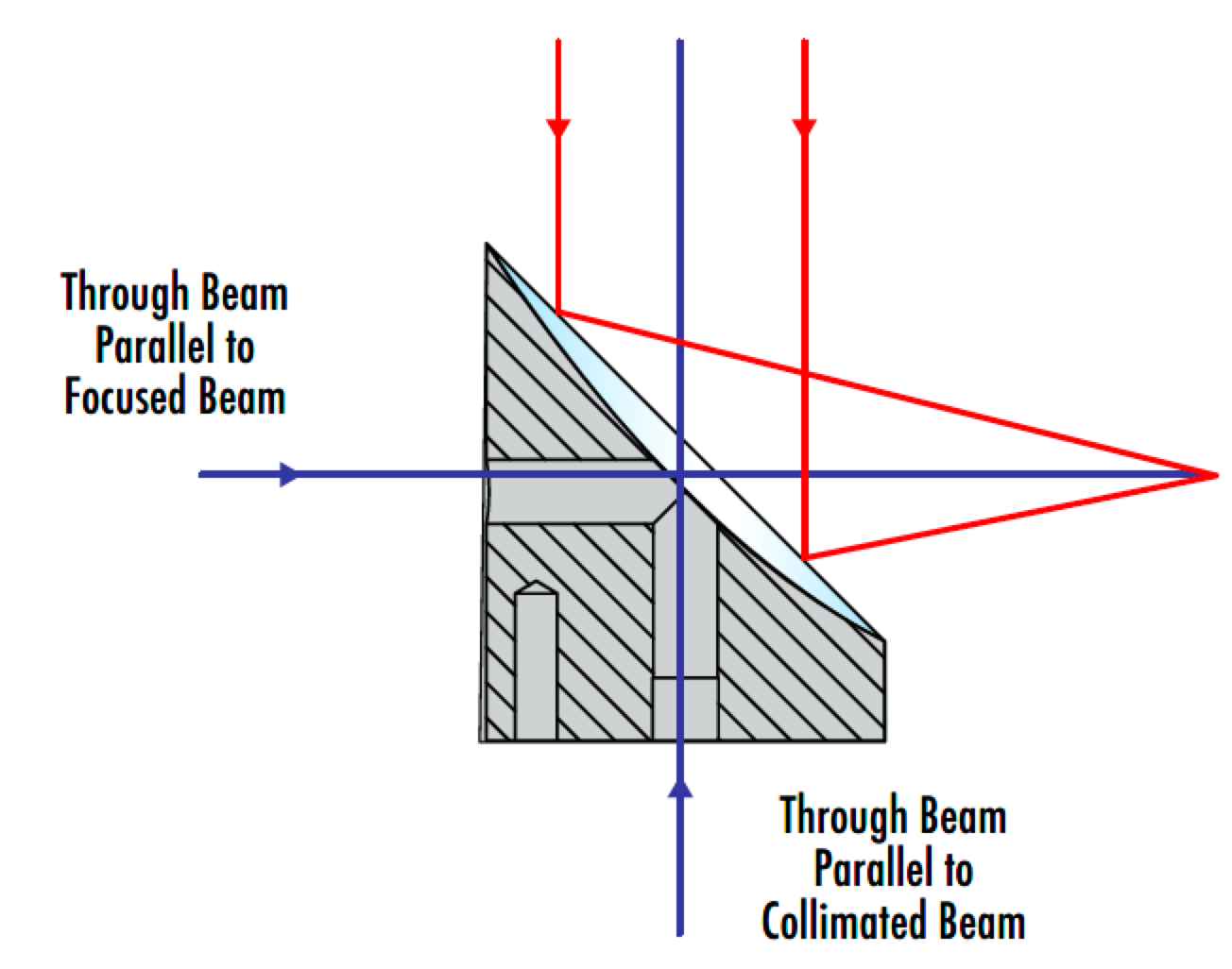
The red light path shown in the figure is to focus the parallel light. Although the far UV is not suitable for the lens, we can still achieve it with a high reflectivity mirror, so we can use parabolic mirrors to focus UV.
And in such an optical path design, a relatively large parabolic mirror is required on the equipment, so it will increase the size of the whole photolithography machine.